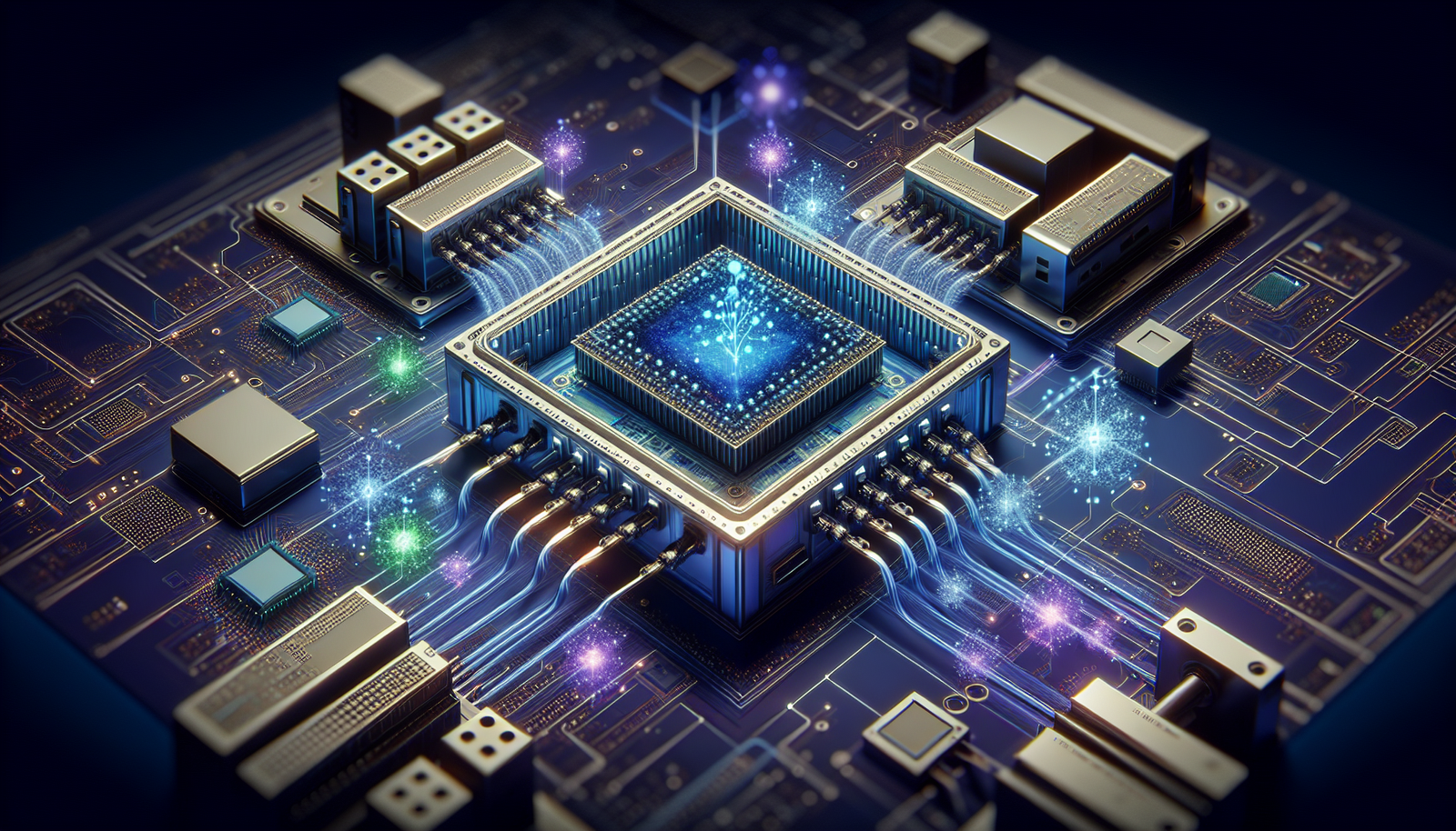
The essor of artificial intelligence (AI) requires high-performance and sustainable infrastructures to process astronomical amounts of data. Traditional methods, relying on graphical processing units (GPUs), struggle to meet these growing demands. The advancement of silicon photonic integrated circuits offers a revolutionary alternative, combining power and efficiency.
*Eliminating energy losses* has become an absolute necessity to propel AI towards future applications. *Adopting a scalable architecture* using optical neural networks could transform the technological landscape. *Optimizing processing speed* while reducing energy costs is a major challenge for innovation.
A revolutionary hardware platform
Recent research has led to a new hardware acceleration platform for artificial intelligence (AI), leveraging photonic integrated circuits on silicon chips. This advancement, led by Dr. Bassem Tossoun, a principal scientist at Hewlett Packard Labs, offers exceptional performance in terms of energy efficiency and scalability.
The current challenges of AI infrastructures
Existing AI infrastructures rely on graphical processing units (GPUs), which present various problems. The demands for high processing power and the resulting energy costs remain critical challenges for their use. Therefore, adopting a more efficient and sustainable AI infrastructure is a promising path for the future development of AI.
Photonic integrated circuits: key advantages
According to a study published in the IEEE Journal of Selected Topics in Quantum Electronics, photonic integrated circuits (PICs) outperform GPU-based architectures in terms of scalability and energy efficiency. By utilizing III-V compound semiconductors, these circuits perform AI workloads more efficiently.
Architecture of neural networks
Photonic accelerators utilize optical neural networks (ONNs), operating at the speed of light with minimal energy loss. Dr. Tossoun emphasizes that, although silicon photonics is easy to manufacture, its scalability for complex integrated circuits remains a challenge. Their platform can serve as a foundation for photonic accelerators with much greater energy efficiency.
Advanced manufacturing process
The fabrication of the devices relied on silicon-on-insulator (SOI) wafers. A complex process including lithography, dry etching, and doping for MOSCAPs and avalanche photodiodes (APDs) has been performed. Selective growth of silicon and germanium has enabled the design of crucial layers for the APDs.
Heterogeneous integration
Heterogeneous integration has enabled the construction of hardware by combining silicon photonics and III-V semiconductors. This approach reduces optical losses while improving the scalability of photonic integrated circuits.
Future prospects for AI
This unique photonic platform allows for the integration of various devices onto a single chip. Active components such as integrated lasers and amplifiers, along with fast detectors, facilitate the development of robust optical neural networks. The materials used generate an energy efficiency 2.9 × 10² times greater than that of other photonic platforms.
Future applications and opportunities
The possibilities offered by this revolutionary technology are changing the landscape of AI and machine learning (ML) applications. Data centers will be capable of processing an increased volume of AI tasks while optimizing energy costs. This advancement addresses many issues of computation and energy, thus enabling sustainable development in this field.
Sources and related studies
To explore these topics further, related studies, such as the introduction of an innovative photonic chip by STMicroelectronics to optimize data centers, also show promising implications in the sector here. Additionally, the blending of photonic neural networks with distributed acoustic sensing for infrastructure monitoring demonstrates the growing integration of photonic technologies in various applications: learn more.
FAQ on leveraging silicon photonics for scalable and sustainable artificial intelligence hardware
What is silicon photonics?
Silicon photonics refers to the use of integrated photonic circuits on silicon chips to manipulate optical signals, thus providing significant advantages in terms of speed and energy efficiency compared to traditional electronic circuits.
How does silicon photonics improve the energy efficiency of artificial intelligence hardware?
Silicon photonics enables operations at the speed of light with minimal energy loss, thereby contributing to reducing the energy costs associated with training artificial intelligence models.
What are the main advantages of photonic integrated circuits compared to graphical processing units (GPUs)?
Photonic integrated circuits are more scalable and energy-efficient than GPUs, allowing for the execution of complex artificial intelligence tasks with significantly reduced energy footprints.
What does heterogeneous integration consist of in the fabrication of photonic devices?
Heterogeneous integration involves the combination of different materials, such as silicon and III-V compound semiconductors, to create efficient and integrated devices, enhancing the performance and density of photonic circuits.
What are the potential applications of silicon photonics in artificial intelligence?
Silicon photonics can be used in various fields, including machine learning, large-scale data processing, and acceleration of analytical algorithms, thereby enabling the development of more advanced AI applications.
What challenges remain to overcome in adopting silicon photonics in existing AI infrastructures?
Major challenges include the scalability of manufacturing, the need for interoperability with existing AI systems, and optimizing performance for varied AI workloads.
What are the environmental impacts of using silicon photonics for artificial intelligence?
The use of silicon photonics could reduce the carbon footprint of data centers due to its lower energy consumption, thus contributing to more sustainable and environmentally friendly technological infrastructures.


